xilinx FPGA FIFO IP核的使用(VHDLISE)

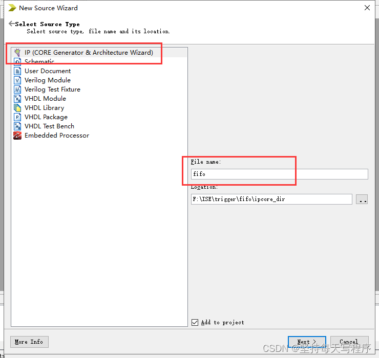
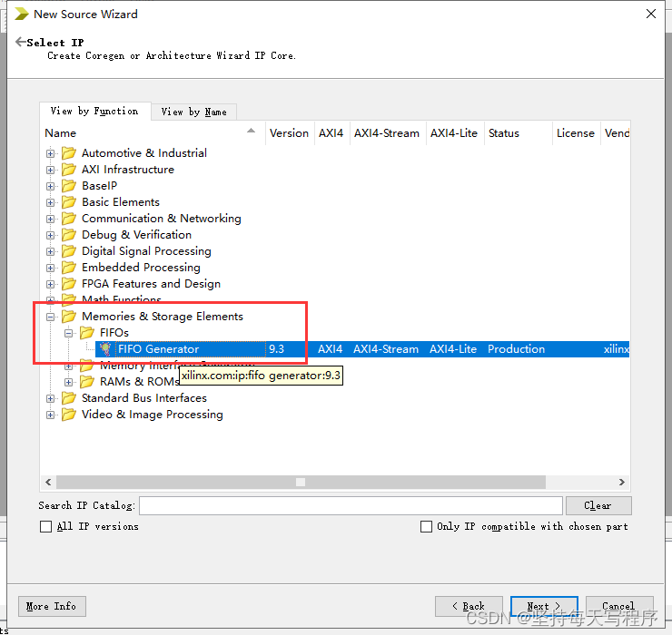
1.新建工程和ip核文件
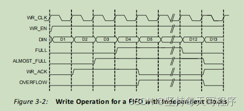
下图显示了一个典型的写操作。拉高WR_EN,导致在WR_CLK的下一个上升边缘发生写入操作。因为FIFO未满,所以WR_ACK输出1,确认成功的写入操作。当只有一个附加的单词可以写入FIFO时,FIFO会拉高ALMOST_FULL标志。当ALMOST_FULL拉高之后,一个附加的写入将导致FIFO拉高FULL。当FULL拉高之后发生写入时,WR_ACK就会为0表示溢出。一旦执行了一个或多个读取操作,FIFO将拉低FULL,并且数据可以成功地写入FIFO,之后WR_ACK也会相应拉高表示溢出取消。
本节描述了FIFO读取操作的行为和相关联的状态标志。当断言读取启用且FIFO不为空时,将从输出总线(DOUT)上的FIFO中读取数据,并断言有效标志(有效)。如果FIFO被连续读取而没有被写入,则FIFO将排空。当FIFO不为空时,读取操作将会成功。当FIFO为空且请求读取时,将忽略读取操作,断言下流标志,且FIFO的状态没有变化(下FIFO是非破坏性的)
读写使用一个时钟时,当写操作和读取操作同时发生时,写操作被接受,读取操作被忽略。
对于Virtex-4 FPGA内置的FIFO实现,全信号有一个额外的延迟周期。使用写确认来验证成功或可编程满的早期指示。
Virtex-4 FPGA内置的FIFO实现在FULL标志上显示了一个额外的延迟周期
Common Clock FIFO: Block RAM and Distributed RAM此实现可选地支持首字切换
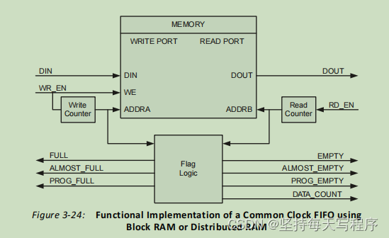
下图说明了一个FIFO的功能实现,使用块RAM或公共RAM的分布式RAM用于内存。所有信号都同步到单个时钟输入(CLK)。这个设计实现了写和读取指针的计数器,用于计算状态标志的逻辑。另外,还有一个可选的同步(SRST)或异步(RST)复位信号。
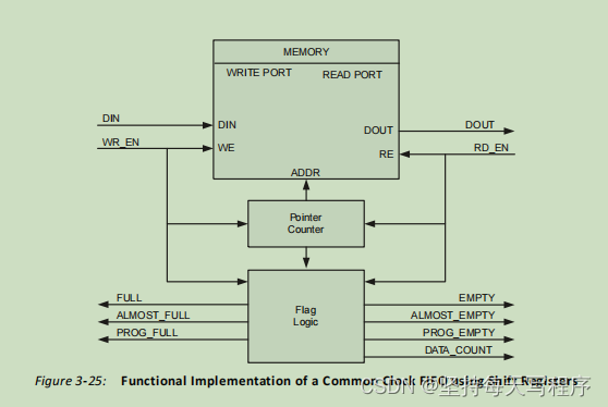
Common Clock FIFO: Shift Registers
此实现仅在Virtex-4 FPGA和更新的架构中可用。
说明了使用移位寄存器配置公共时钟的FIFO的功能实现。所有操作都同步到同一时钟输入(CLK)。这个设计实现了一个写和读指针和逻辑的上/下计数器,用于计算状态标志的逻辑。
Common Clock (CLK), Built-in FIFO(独立时钟,内置fifo)
此实现可选地支持第一个字的故障切换
FIFO生成器支持使用内置的FIFO原语的FIFO内核。这为用户提供了使用内置的FIFO的能力,而只需要一个时钟接口。具有内置FIFO的公共时钟配置的行为与具有内置FIFO的独立时钟配置相同,除了所有操作都与公共时钟(CLK)有关。
此实现可选地支持非对称读/写端口和第一个字的故障切换
说明了一个配置了独立时钟的FIFO的功能实现。这个实现使用块RAM或分布式RAM用于内存,用于写和读指针的计数器,二进制代码和灰度代码之间的转换用于跨时钟域的同步,以及用于计算状态标志的逻辑。
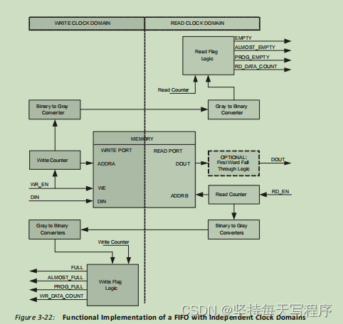
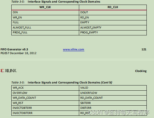
该FIFO被设计为支持一个独立的读时钟(RD_CLK)和写时钟(WR_CLK);换句话说,RD_CLK和WR_CLK之间的频率或相位没有必要的关系。下表总结了FIFO接口信号,它们仅在各自的时钟域中有效
对于使用独立时钟的FIFO核心,写操作和读取操作与状态标志之间的时间关系受到两个时钟之间关系的影响。例如,写入空FIFO和断空之间的时间由写时钟和读时钟之间的相位和频率关系决定。
我选择了读写独立时钟,配置成内部fifo

read mode
读取模式仅在选择块RAM或分布式RAM FIFOs时可用。对内置FIFOs的支持仅适用于Kintex-7、Virtex-7、Virtex-6和Virtex-5的FPGA实现。
标准FIFO实现了具有标准延迟的FIFO,而不使用输出寄存器。
第一字下降直通FIFO实现了一个具有注册输出的FIFO。
--------------------------------------------------------------------------------
-- Company:
-- Engineer:
--
-- Create Date:   14:37:40 09/01/2022
-- Design Name:
-- Module Name:   F:/ISE/trigger/fifo/fifo_tb.vhd
-- Project Name:  fifo
-- Target Device:
-- Tool versions:
-- Description:
--
-- VHDL Test Bench Created by ISE for module: fifo
--
-- Dependencies:
--
-- Revision:
-- Revision 0.01 - File Created
-- Additional Comments:
--
-- Notes:
-- This testbench has been automatically generated using types std_logic and
-- std_logic_vector for the ports of the unit under test.  Xilinx recommends
-- that these types always be used for the top-level I/O of a design in order
-- to guarantee that the testbench will bind correctly to the post-implementation
-- simulation model.
--------------------------------------------------------------------------------
LIBRARY ieee;
USE ieee.std_logic_1164.ALL;use ieee.std_logic_unsigned.all;
use ieee.std_logic_arith.all;
-- Uncomment the following library declaration if using
-- arithmetic functions with Signed or Unsigned values
--USE ieee.numeric_std.ALL;ENTITY fifo_tb IS
END fifo_tb;ARCHITECTURE behavior OF fifo_tb IS -- Component Declaration for the Unit Under Test (UUT)COMPONENT fifoPORT (rst : IN STD_LOGIC;wr_clk : IN STD_LOGIC;rd_clk : IN STD_LOGIC;din : IN STD_LOGIC_VECTOR(17 DOWNTO 0);wr_en : IN STD_LOGIC;rd_en : IN STD_LOGIC;dout : OUT STD_LOGIC_VECTOR(17 DOWNTO 0);full : OUT STD_LOGIC;almost_full : OUT STD_LOGIC;wr_ack : OUT STD_LOGIC;overflow : OUT STD_LOGIC;empty : OUT STD_LOGIC;almost_empty : OUT STD_LOGIC;valid : OUT STD_LOGIC;underflow : OUT STD_LOGIC;rd_data_count : OUT STD_LOGIC_VECTOR(8 DOWNTO 0);wr_data_count : OUT STD_LOGIC_VECTOR(8 DOWNTO 0));
END COMPONENT;--Inputssignal rst : std_logic := '0';signal wr_clk : std_logic := '0';signal rd_clk : std_logic := '0';signal din : std_logic_vector(17 downto 0) := (others => '0');signal wr_en : std_logic := '0';signal rd_en : std_logic := '0';--Outputssignal dout : std_logic_vector(17 downto 0):= (others => '0');signal full : std_logic:= '0';signal empty : std_logic:= '0';signal valid : std_logic:= '0';signal underflow : std_logic:= '0';signal rd_data_count : std_logic_vector(8 downto 0):= (others => '0');signal wr_data_count : std_logic_vector(8 downto 0):= (others => '0');signal almost_full : std_logic:= '0';signal wr_ack : std_logic:= '0';signal overflow : std_logic:= '0';signal almost_empty : std_logic:= '0';-- Clock period definitionsconstant wr_clk_period : time := 10 ns;constant rd_clk_period : time := 10 ns;BEGIN-- Instantiate the Unit Under Test (UUT)uut: fifo PORT MAP (rst => rst,wr_clk => wr_clk,rd_clk => rd_clk,din => din,wr_en => wr_en,rd_en => rd_en,dout => dout,full => full,almost_full => almost_full,wr_ack => wr_ack,overflow => overflow,empty => empty,almost_empty => almost_empty,valid => valid,underflow => underflow,rd_data_count => rd_data_count,wr_data_count => wr_data_count);-- Clock process definitionswr_clk_process :processbeginwr_clk <= '0';wait for wr_clk_period/2;wr_clk <= '1';wait for wr_clk_period/2;end process;rd_clk_process :processbeginrd_clk <= '0';wait for rd_clk_period/2;rd_clk <= '1';wait for rd_clk_period/2;end process;-- Stimulus processstim_proc: processbegin		rst <= '1';wr_en <= '0';rd_en <= '0'; din <= (others => '0');wait for wr_clk_period;rst <= '0';wait for wr_clk_period*5;wr_en <= '1'; din <= "00"&X"1203";wait for wr_clk_period;wr_en <= '0';wait for wr_clk_period*10;rd_en <= '1';   wr_en <= '1'; din <= "00"&X"1103";wait for wr_clk_period;wr_en <= '0';rd_en <= '0';wait for wr_clk_period*10;rd_en <= '1';  wr_en <= '1'; din <= "10"&X"1103";wait for wr_clk_period;wr_en <= '0';rd_en <= '0';wait for wr_clk_period*10;rd_en <= '1';  wr_en <= '1'; din <= "01"&X"1103";wait for wr_clk_period;wr_en <= '0';rd_en <= '0';wait for wr_clk_period*10;-- insert stimulus here wait;end process;END;
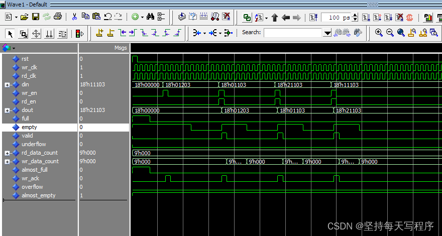
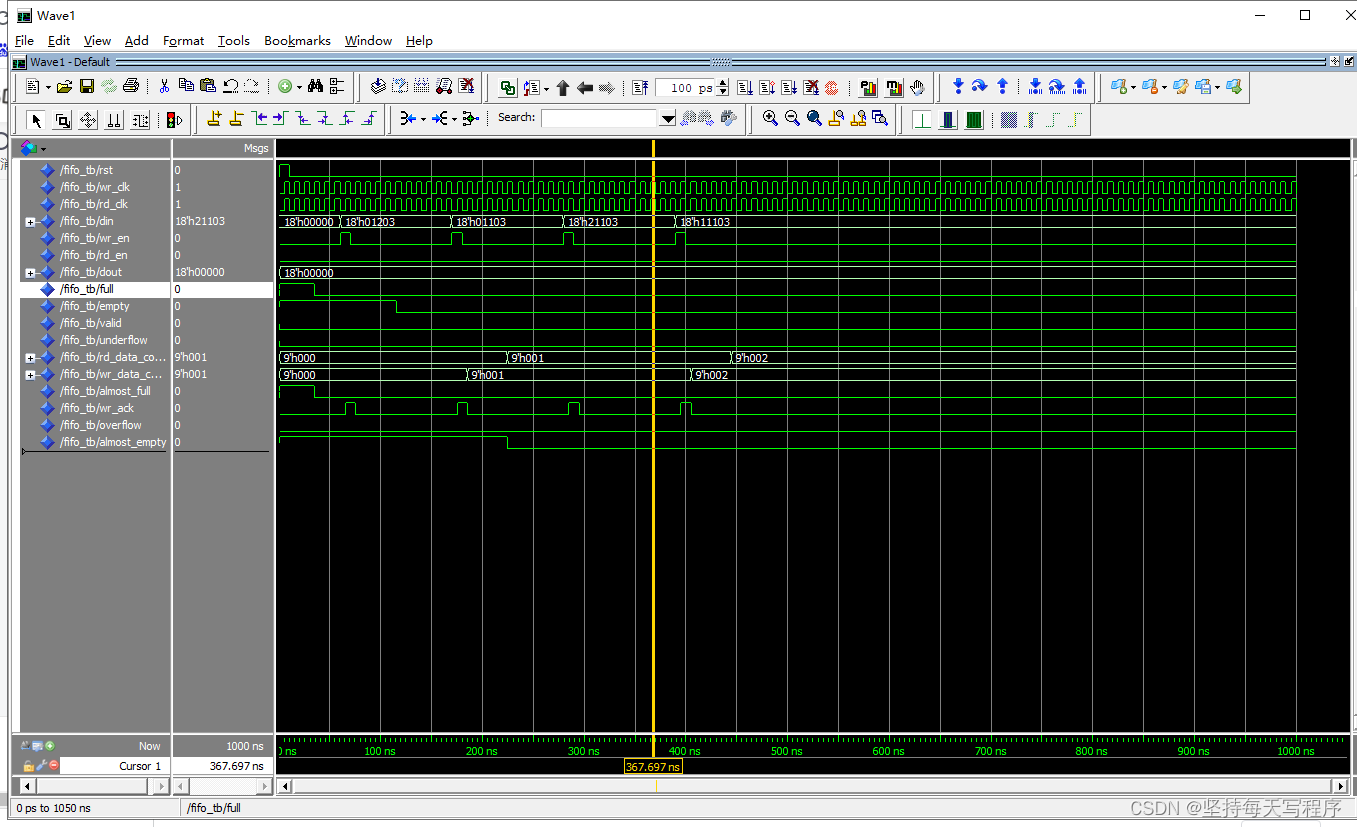
先写再读,而且是写一个之后就开始读,并且读写频率一样,所以仿真结果就是写一次读一次
--------------------------------------------------------------------------------
-- Company:
-- Engineer:
--
-- Create Date:   14:37:40 09/01/2022
-- Design Name:
-- Module Name:   F:/ISE/trigger/fifo/fifo_tb.vhd
-- Project Name:  fifo
-- Target Device:
-- Tool versions:
-- Description:
--
-- VHDL Test Bench Created by ISE for module: fifo
--
-- Dependencies:
--
-- Revision:
-- Revision 0.01 - File Created
-- Additional Comments:
--
-- Notes:
-- This testbench has been automatically generated using types std_logic and
-- std_logic_vector for the ports of the unit under test.  Xilinx recommends
-- that these types always be used for the top-level I/O of a design in order
-- to guarantee that the testbench will bind correctly to the post-implementation
-- simulation model.
--------------------------------------------------------------------------------
LIBRARY ieee;
USE ieee.std_logic_1164.ALL;use ieee.std_logic_unsigned.all;
use ieee.std_logic_arith.all;
-- Uncomment the following library declaration if using
-- arithmetic functions with Signed or Unsigned values
--USE ieee.numeric_std.ALL;ENTITY fifo_tb IS
END fifo_tb;ARCHITECTURE behavior OF fifo_tb IS -- Component Declaration for the Unit Under Test (UUT)COMPONENT fifoPORT (rst : IN STD_LOGIC;wr_clk : IN STD_LOGIC;rd_clk : IN STD_LOGIC;din : IN STD_LOGIC_VECTOR(17 DOWNTO 0);wr_en : IN STD_LOGIC;rd_en : IN STD_LOGIC;dout : OUT STD_LOGIC_VECTOR(17 DOWNTO 0);full : OUT STD_LOGIC;almost_full : OUT STD_LOGIC;wr_ack : OUT STD_LOGIC;overflow : OUT STD_LOGIC;empty : OUT STD_LOGIC;almost_empty : OUT STD_LOGIC;valid : OUT STD_LOGIC;underflow : OUT STD_LOGIC;rd_data_count : OUT STD_LOGIC_VECTOR(8 DOWNTO 0);wr_data_count : OUT STD_LOGIC_VECTOR(8 DOWNTO 0));
END COMPONENT;--Inputssignal rst : std_logic := '0';signal wr_clk : std_logic := '0';signal rd_clk : std_logic := '0';signal din : std_logic_vector(17 downto 0) := (others => '0');signal wr_en : std_logic := '0';signal rd_en : std_logic := '0';--Outputssignal dout : std_logic_vector(17 downto 0):= (others => '0');signal full : std_logic:= '0';signal empty : std_logic:= '0';signal valid : std_logic:= '0';signal underflow : std_logic:= '0';signal rd_data_count : std_logic_vector(8 downto 0):= (others => '0');signal wr_data_count : std_logic_vector(8 downto 0):= (others => '0');signal almost_full : std_logic:= '0';signal wr_ack : std_logic:= '0';signal overflow : std_logic:= '0';signal almost_empty : std_logic:= '0';-- Clock period definitionsconstant wr_clk_period : time := 10 ns;constant rd_clk_period : time := 10 ns;BEGIN-- Instantiate the Unit Under Test (UUT)uut: fifo PORT MAP (rst => rst,wr_clk => wr_clk,rd_clk => rd_clk,din => din,wr_en => wr_en,rd_en => rd_en,dout => dout,full => full,almost_full => almost_full,wr_ack => wr_ack,overflow => overflow,empty => empty,almost_empty => almost_empty,valid => valid,underflow => underflow,rd_data_count => rd_data_count,wr_data_count => wr_data_count);-- Clock process definitionswr_clk_process :processbeginwr_clk <= '0';wait for wr_clk_period/2;wr_clk <= '1';wait for wr_clk_period/2;end process;rd_clk_process :processbeginrd_clk <= '0';wait for rd_clk_period/2;rd_clk <= '1';wait for rd_clk_period/2;end process;-- Stimulus processstim_proc: processbegin		rst <= '1';wr_en <= '0';rd_en <= '0'; din <= (others => '0');wait for wr_clk_period;rst <= '0';wait for wr_clk_period*5;wr_en <= '1'; din <= "00"&X"1203";wait for wr_clk_period;wr_en <= '0';wait for wr_clk_period*3;rd_en <= '1';   wr_en <= '1'; din <= "00"&X"1103";wait for wr_clk_period;wr_en <= '0';wait for wr_clk_period*3;wr_en <= '1'; din <= "10"&X"1103";wait for wr_clk_period;wr_en <= '0';wait for wr_clk_period*3;wr_en <= '1'; din <= "01"&X"1103";wait for wr_clk_period;wr_en <= '0';wait for wr_clk_period*3;-- insert stimulus here wait;end process;END;
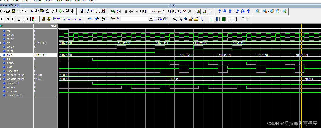
先写两个数据,再读,所以读出的结果就是当读使能来的时候,立马读出两个数,然后再去等待下一个数写入
-- Stimulus processstim_proc: processbegin rst <= '1';wr_en <= '0';rd_en <= '0'; din <= (others => '0');wait for wr_clk_period;rst <= '0';wait for wr_clk_period*5;wr_en <= '1'; din <= "00"&X"1203";wait for wr_clk_period;wr_en <= '0';wait for wr_clk_period*3;wr_en <= '1'; din <= "00"&X"1103";wait for wr_clk_period;wr_en <= '0';wait for wr_clk_period*3;rd_en <= '1'; wr_en <= '1'; din <= "10"&X"1103";wait for wr_clk_period;wr_en <= '0';wait for wr_clk_period*3;wr_en <= '1'; din <= "01"&X"1103";wait for wr_clk_period;wr_en <= '0';wait for wr_clk_period*3;-- insert stimulus here wait;end process;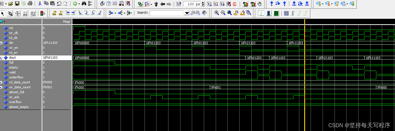
这次是先使能读,然后再写,就会等数据写进去之后,数据才会读出
-- Stimulus processstim_proc: processbegin rst <= '1';wr_en <= '0';rd_en <= '0'; din <= (others => '0');wait for wr_clk_period;rst <= '0';wait for wr_clk_period*5;rd_en <= '1'; wait for wr_clk_period*5;wr_en <= '1'; din <= "00"&X"1203";wait for wr_clk_period;wr_en <= '0';wait for wr_clk_period*3;wr_en <= '1'; din <= "00"&X"1103";wait for wr_clk_period;wr_en <= '0';wait for wr_clk_period*3;wr_en <= '1'; din <= "10"&X"1103";wait for wr_clk_period;wr_en <= '0';wait for wr_clk_period*3;wr_en <= '1'; din <= "01"&X"1103";wait for wr_clk_period;wr_en <= '0';wait for wr_clk_period*3;-- insert stimulus here wait;end process;
测试结论就是,用fifo读写可以避免用rom,因为数据还没有写入时,一直读出上一次的数据,用fifo就可以在vaild为高时去读取,这样读出的数就是依次写入的数据