11、STM32H7 MPU Cache

篇前小问题
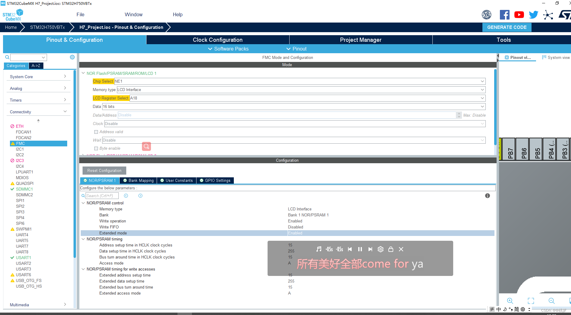
在使用stm32H750的FMC时,出现一些奇怪的问题,写A时序时时,总是写1次的代码了出现了写四次的时序,所以找了很久,才找到问题出在了MPU上,使用FMC时,必须开启MPU,不然会出现此现象。
while一直执行该函数,会出现此时序图:
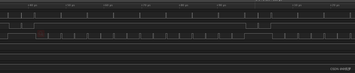
读时序是两字节,但是写出现的时序明显异常
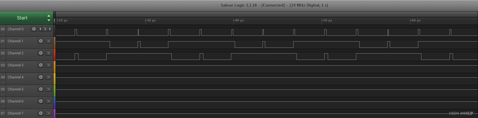
经过解决,才出现正常的时序,如下所示
解决方法:
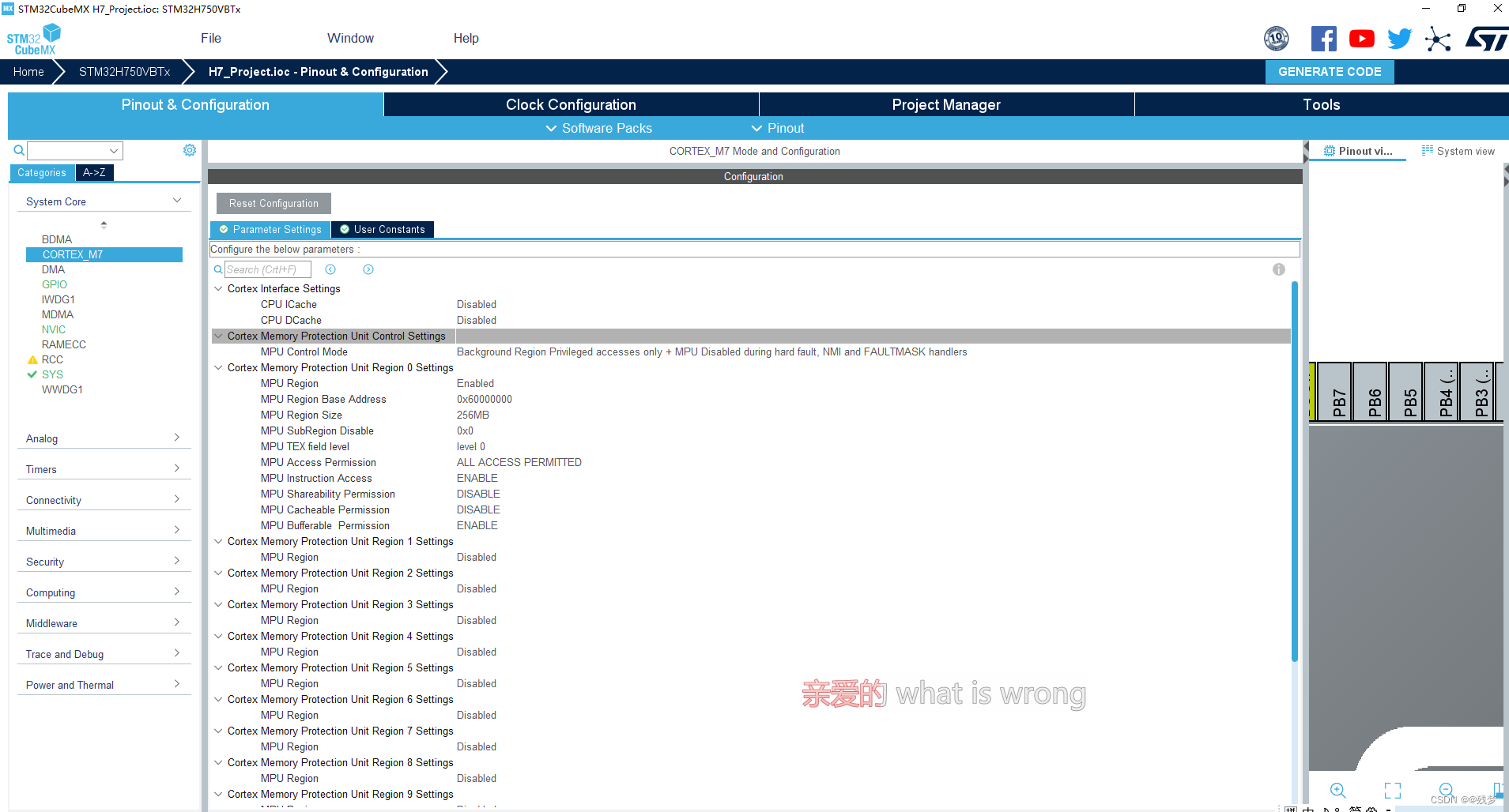
开启FMC的区域保护:
void MPU_Config(void)
{MPU_Region_InitTypeDef MPU_InitStruct = {0};/* Disables the MPU */HAL_MPU_Disable();/ Initializes and configures the Region and the memory to be protected*/MPU_InitStruct.Enable = MPU_REGION_ENABLE;MPU_InitStruct.Number = MPU_REGION_NUMBER0;MPU_InitStruct.BaseAddress = 0x60000000;MPU_InitStruct.Size = MPU_REGION_SIZE_256MB;MPU_InitStruct.SubRegionDisable = 0x0;MPU_InitStruct.TypeExtField = MPU_TEX_LEVEL0;MPU_InitStruct.AccessPermission = MPU_REGION_FULL_ACCESS;MPU_InitStruct.DisableExec = MPU_INSTRUCTION_ACCESS_ENABLE;MPU_InitStruct.IsShareable = MPU_ACCESS_NOT_SHAREABLE;MPU_InitStruct.IsCacheable = MPU_ACCESS_NOT_CACHEABLE;MPU_InitStruct.IsBufferable = MPU_ACCESS_BUFFERABLE;HAL_MPU_ConfigRegion(&MPU_InitStruct);/* Enables the MPU */HAL_MPU_Enable(MPU_HFNMI_PRIVDEF);}
同样问题经验贴参考:https://www.stmcu.org.cn/module/forum/forum.php?mod=viewthread&tid=623865&page=1#pid2491693
至于为什么非要开启MPU呢,因为
参考出处:https://www.armbbs.cn/forum.php?mod=viewthread&tid=89929
说了这么多,先发下代码吧:
fmc.c
/* File Name : FMC.c* Description : This file provides code for the configuration* of the FMC peripheral.* @attention <h2><center>© Copyright (c) 2023 STMicroelectronics.* All rights reserved.</center></h2> This software component is licensed by ST under Ultimate Liberty license* SLA0044, the "License"; You may not use this file except in compliance with* the License. You may obtain a copy of the License at:* www.st.com/SLA0044//* Includes ------------------------------------------------------------------*/
#include "fmc.h"/* USER CODE BEGIN 0 */
/* USER CODE END 0 */SRAM_HandleTypeDef hsram1;/* FMC initialization function */
void MX_FMC_Init(void)
{/* USER CODE BEGIN FMC_Init 0 *//* USER CODE END FMC_Init 0 */FMC_NORSRAM_TimingTypeDef Timing = {0};FMC_NORSRAM_TimingTypeDef ExtTiming = {0};/* USER CODE BEGIN FMC_Init 1 *//* USER CODE END FMC_Init 1 *// Perform the SRAM1 memory initialization sequence*/hsram1.Instance = FMC_NORSRAM_DEVICE;hsram1.Extended = FMC_NORSRAM_EXTENDED_DEVICE;/* hsram1.Init */hsram1.Init.NSBank = FMC_NORSRAM_BANK1;hsram1.Init.DataAddressMux = FMC_DATA_ADDRESS_MUX_DISABLE;hsram1.Init.MemoryType = FMC_MEMORY_TYPE_SRAM;hsram1.Init.MemoryDataWidth = FMC_NORSRAM_MEM_BUS_WIDTH_16;hsram1.Init.BurstAccessMode = FMC_BURST_ACCESS_MODE_DISABLE;hsram1.Init.WaitSignalPolarity = FMC_WAIT_SIGNAL_POLARITY_LOW;hsram1.Init.WaitSignalActive = FMC_WAIT_TIMING_BEFORE_WS;hsram1.Init.WriteOperation = FMC_WRITE_OPERATION_ENABLE;hsram1.Init.WaitSignal = FMC_WAIT_SIGNAL_DISABLE;hsram1.Init.ExtendedMode = FMC_EXTENDED_MODE_ENABLE;hsram1.Init.AsynchronousWait = FMC_ASYNCHRONOUS_WAIT_DISABLE;hsram1.Init.WriteBurst = FMC_WRITE_BURST_DISABLE;hsram1.Init.ContinuousClock = FMC_CONTINUOUS_CLOCK_SYNC_ONLY;hsram1.Init.WriteFifo = FMC_WRITE_FIFO_DISABLE;hsram1.Init.PageSize = FMC_PAGE_SIZE_NONE;/* Timing */Timing.AddressSetupTime = 15;Timing.AddressHoldTime = 15;Timing.DataSetupTime = 255;Timing.BusTurnAroundDuration = 15;Timing.CLKDivision = 16;Timing.DataLatency = 17;Timing.AccessMode = FMC_ACCESS_MODE_A;/* ExtTiming */ExtTiming.AddressSetupTime = 15;ExtTiming.AddressHoldTime = 15;ExtTiming.DataSetupTime = 255;ExtTiming.BusTurnAroundDuration = 15;ExtTiming.CLKDivision = 16;ExtTiming.DataLatency = 17;ExtTiming.AccessMode = FMC_ACCESS_MODE_A;if (HAL_SRAM_Init(&hsram1, &Timing, &ExtTiming) != HAL_OK){Error_Handler( );}/* USER CODE BEGIN FMC_Init 2 *//* USER CODE END FMC_Init 2 */
}static uint32_t FMC_Initialized = 0;static void HAL_FMC_MspInit(void){/* USER CODE BEGIN FMC_MspInit 0 *//* USER CODE END FMC_MspInit 0 */GPIO_InitTypeDef GPIO_InitStruct = {0};if (FMC_Initialized) {return;}FMC_Initialized = 1;RCC_PeriphCLKInitTypeDef PeriphClkInitStruct = {0};/ Initializes the peripherals clock*/PeriphClkInitStruct.PeriphClockSelection = RCC_PERIPHCLK_FMC;PeriphClkInitStruct.PLL2.PLL2M = 8;PeriphClkInitStruct.PLL2.PLL2N = 20;PeriphClkInitStruct.PLL2.PLL2P = 2;PeriphClkInitStruct.PLL2.PLL2Q = 2;PeriphClkInitStruct.PLL2.PLL2R = 2;PeriphClkInitStruct.PLL2.PLL2RGE = RCC_PLL2VCIRANGE_3;PeriphClkInitStruct.PLL2.PLL2VCOSEL = RCC_PLL2VCOMEDIUM;PeriphClkInitStruct.FmcClockSelection = RCC_FMCCLKSOURCE_PLL2;if (HAL_RCCEx_PeriphCLKConfig(&PeriphClkInitStruct) != HAL_OK){Error_Handler();}/* Peripheral clock enable */__HAL_RCC_FMC_CLK_ENABLE();/ FMC GPIO ConfigurationPE7 ------> FMC_D4PE8 ------> FMC_D5PE9 ------> FMC_D6PE10 ------> FMC_D7PE11 ------> FMC_D8PE12 ------> FMC_D9PE13 ------> FMC_D10PE14 ------> FMC_D11PE15 ------> FMC_D12PD8 ------> FMC_D13PD9 ------> FMC_D14PD10 ------> FMC_D15PD13 ------> FMC_A18PD14 ------> FMC_D0PD15 ------> FMC_D1PC7 ------> FMC_NE1PD0 ------> FMC_D2PD1 ------> FMC_D3PD4 ------> FMC_NOEPD5 ------> FMC_NWE*//* GPIO_InitStruct */GPIO_InitStruct.Pin = GPIO_PIN_7|GPIO_PIN_8|GPIO_PIN_9|GPIO_PIN_10|GPIO_PIN_11|GPIO_PIN_12|GPIO_PIN_13|GPIO_PIN_14|GPIO_PIN_15;GPIO_InitStruct.Mode = GPIO_MODE_AF_PP;GPIO_InitStruct.Pull = GPIO_NOPULL;GPIO_InitStruct.Speed = GPIO_SPEED_FREQ_VERY_HIGH;GPIO_InitStruct.Alternate = GPIO_AF12_FMC;HAL_GPIO_Init(GPIOE, &GPIO_InitStruct);/* GPIO_InitStruct */GPIO_InitStruct.Pin = GPIO_PIN_8|GPIO_PIN_9|GPIO_PIN_10|GPIO_PIN_13|GPIO_PIN_14|GPIO_PIN_15|GPIO_PIN_0|GPIO_PIN_1|GPIO_PIN_4|GPIO_PIN_5;GPIO_InitStruct.Mode = GPIO_MODE_AF_PP;GPIO_InitStruct.Pull = GPIO_NOPULL;GPIO_InitStruct.Speed = GPIO_SPEED_FREQ_VERY_HIGH;GPIO_InitStruct.Alternate = GPIO_AF12_FMC;HAL_GPIO_Init(GPIOD, &GPIO_InitStruct);/* GPIO_InitStruct */GPIO_InitStruct.Pin = GPIO_PIN_7;GPIO_InitStruct.Mode = GPIO_MODE_AF_PP;GPIO_InitStruct.Pull = GPIO_NOPULL;GPIO_InitStruct.Speed = GPIO_SPEED_FREQ_VERY_HIGH;GPIO_InitStruct.Alternate = GPIO_AF9_FMC;HAL_GPIO_Init(GPIOC, &GPIO_InitStruct);/* USER CODE BEGIN FMC_MspInit 1 *//* USER CODE END FMC_MspInit 1 */
}void HAL_SRAM_MspInit(SRAM_HandleTypeDef* sramHandle){/* USER CODE BEGIN SRAM_MspInit 0 *//* USER CODE END SRAM_MspInit 0 */HAL_FMC_MspInit();/* USER CODE BEGIN SRAM_MspInit 1 *//* USER CODE END SRAM_MspInit 1 */
}static uint32_t FMC_DeInitialized = 0;static void HAL_FMC_MspDeInit(void){/* USER CODE BEGIN FMC_MspDeInit 0 *//* USER CODE END FMC_MspDeInit 0 */if (FMC_DeInitialized) {return;}FMC_DeInitialized = 1;/* Peripheral clock enable */__HAL_RCC_FMC_CLK_DISABLE();/ FMC GPIO ConfigurationPE7 ------> FMC_D4PE8 ------> FMC_D5PE9 ------> FMC_D6PE10 ------> FMC_D7PE11 ------> FMC_D8PE12 ------> FMC_D9PE13 ------> FMC_D10PE14 ------> FMC_D11PE15 ------> FMC_D12PD8 ------> FMC_D13PD9 ------> FMC_D14PD10 ------> FMC_D15PD13 ------> FMC_A18PD14 ------> FMC_D0PD15 ------> FMC_D1PC7 ------> FMC_NE1PD0 ------> FMC_D2PD1 ------> FMC_D3PD4 ------> FMC_NOEPD5 ------> FMC_NWE*/HAL_GPIO_DeInit(GPIOE, GPIO_PIN_7|GPIO_PIN_8|GPIO_PIN_9|GPIO_PIN_10|GPIO_PIN_11|GPIO_PIN_12|GPIO_PIN_13|GPIO_PIN_14|GPIO_PIN_15);HAL_GPIO_DeInit(GPIOD, GPIO_PIN_8|GPIO_PIN_9|GPIO_PIN_10|GPIO_PIN_13|GPIO_PIN_14|GPIO_PIN_15|GPIO_PIN_0|GPIO_PIN_1|GPIO_PIN_4|GPIO_PIN_5);HAL_GPIO_DeInit(GPIOC, GPIO_PIN_7);/* USER CODE BEGIN FMC_MspDeInit 1 *//* USER CODE END FMC_MspDeInit 1 */
}void HAL_SRAM_MspDeInit(SRAM_HandleTypeDef* sramHandle){/* USER CODE BEGIN SRAM_MspDeInit 0 *//* USER CODE END SRAM_MspDeInit 0 */HAL_FMC_MspDeInit();/* USER CODE BEGIN SRAM_MspDeInit 1 *//* USER CODE END SRAM_MspDeInit 1 */
}
/* @}*//* @}*// (C) COPYRIGHT STMicroelectronics *END OF FILE/main.c
/* USER CODE BEGIN Header */
/* @file : main.c* @brief : Main program body* @attention <h2><center>© Copyright (c) 2023 STMicroelectronics.* All rights reserved.</center></h2> This software component is licensed by ST under Ultimate Liberty license* SLA0044, the "License"; You may not use this file except in compliance with* the License. You may obtain a copy of the License at:* www.st.com/SLA0044/
/* USER CODE END Header */
/* Includes ------------------------------------------------------------------*/
#include "main.h"
#include "fatfs.h"
#include "sdmmc.h"
#include "tim.h"
#include "usart.h"
#include "gpio.h"
#include "fmc.h"/* Private includes ----------------------------------------------------------*/
/* USER CODE BEGIN Includes */
#include "Common_Driver.h"
#include "sdCheck.h"
#include "Key_Driver.h"
/* USER CODE END Includes *//* Private typedef -----------------------------------------------------------*/
/* USER CODE BEGIN PTD *//* USER CODE END PTD *//* Private define ------------------------------------------------------------*/
/* USER CODE BEGIN PD */
/* USER CODE END PD *//* Private macro -------------------------------------------------------------*/
/* USER CODE BEGIN PM *//* USER CODE END PM *//* Private variables ---------------------------------------------------------*//* USER CODE BEGIN PV *//* USER CODE END PV *//* Private function prototypes -----------------------------------------------*/
void SystemClock_Config(void);
static void MPU_Config(void);
/* USER CODE BEGIN PFP *//* USER CODE END PFP *//* Private user code ---------------------------------------------------------*/
/* USER CODE BEGIN 0 */
typedef struct
{volatile uint16_t LCD_REG;volatile uint16_t LCD_RAM;
} LCD_TypeDef;#define LCD_BASE ((uint32_t)(0x60000000 | 0x0007FFFE))
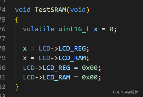
#define LCD ((LCD_TypeDef *) LCD_BASE)void TestSRAM(void)
{volatile uint16_t x = 0;x = LCD->LCD_REG;x = LCD->LCD_RAM;LCD->LCD_REG = 0x00;LCD->LCD_RAM = 0x00;
}/* USER CODE END 0 *//* @brief The application entry point.* @retval int*/
int main(void)
{/* USER CODE BEGIN 1 */extern uint8_t KeyFlag[2];/* USER CODE END 1 *//* MPU Configuration--------------------------------------------------------*/MPU_Config();/* MCU Configuration--------------------------------------------------------*//* Reset of all peripherals, Initializes the Flash interface and the Systick. */HAL_Init();/* USER CODE BEGIN Init *//* USER CODE END Init *//* Configure the system clock */SystemClock_Config();/* USER CODE BEGIN SysInit *///MPU_Configx();/* USER CODE END SysInit *//* Initialize all configured peripherals */MX_GPIO_Init();MX_USART1_UART_Init();MX_SDMMC1_SD_Init();MX_FATFS_Init();MX_TIM17_Init();MX_FMC_Init();/* USER CODE BEGIN 2 */sdCheck_Init();Key_Init();//HAL_TIM_Base_Start_IT(&htim17);//1ms任务,需在服务器之前启动HAL_Delay(1);/* USER CODE END 2 *//* Infinite loop *//* USER CODE BEGIN WHILE */while (1){/* USER CODE END WHILE *//* USER CODE BEGIN 3 */TestSRAM();}/* USER CODE END 3 */
}/* @brief System Clock Configuration* @retval None*/
void SystemClock_Config(void)
{RCC_OscInitTypeDef RCC_OscInitStruct = {0};RCC_ClkInitTypeDef RCC_ClkInitStruct = {0};/ Supply configuration update enable*/HAL_PWREx_ConfigSupply(PWR_LDO_SUPPLY);/ Configure the main internal regulator output voltage*/__HAL_PWR_VOLTAGESCALING_CONFIG(PWR_REGULATOR_VOLTAGE_SCALE0);while(!__HAL_PWR_GET_FLAG(PWR_FLAG_VOSRDY)) {}/ Macro to configure the PLL clock source*/__HAL_RCC_PLL_PLLSOURCE_CONFIG(RCC_PLLSOURCE_HSI);/ Initializes the RCC Oscillators according to the specified parameters* in the RCC_OscInitTypeDef structure.*/RCC_OscInitStruct.OscillatorType = RCC_OSCILLATORTYPE_HSI;RCC_OscInitStruct.HSIState = RCC_HSI_DIV1;RCC_OscInitStruct.HSICalibrationValue = RCC_HSICALIBRATION_DEFAULT;RCC_OscInitStruct.PLL.PLLState = RCC_PLL_ON;RCC_OscInitStruct.PLL.PLLSource = RCC_PLLSOURCE_HSI;RCC_OscInitStruct.PLL.PLLM = 4;RCC_OscInitStruct.PLL.PLLN = 60;RCC_OscInitStruct.PLL.PLLP = 2;RCC_OscInitStruct.PLL.PLLQ = 20;RCC_OscInitStruct.PLL.PLLR = 2;RCC_OscInitStruct.PLL.PLLRGE = RCC_PLL1VCIRANGE_3;RCC_OscInitStruct.PLL.PLLVCOSEL = RCC_PLL1VCOWIDE;RCC_OscInitStruct.PLL.PLLFRACN = 0;if (HAL_RCC_OscConfig(&RCC_OscInitStruct) != HAL_OK){Error_Handler();}/ Initializes the CPU, AHB and APB buses clocks*/RCC_ClkInitStruct.ClockType = RCC_CLOCKTYPE_HCLK|RCC_CLOCKTYPE_SYSCLK|RCC_CLOCKTYPE_PCLK1|RCC_CLOCKTYPE_PCLK2|RCC_CLOCKTYPE_D3PCLK1|RCC_CLOCKTYPE_D1PCLK1;RCC_ClkInitStruct.SYSCLKSource = RCC_SYSCLKSOURCE_PLLCLK;RCC_ClkInitStruct.SYSCLKDivider = RCC_SYSCLK_DIV1;RCC_ClkInitStruct.AHBCLKDivider = RCC_HCLK_DIV2;RCC_ClkInitStruct.APB3CLKDivider = RCC_APB3_DIV2;RCC_ClkInitStruct.APB1CLKDivider = RCC_APB1_DIV2;RCC_ClkInitStruct.APB2CLKDivider = RCC_APB2_DIV2;RCC_ClkInitStruct.APB4CLKDivider = RCC_APB4_DIV2;if (HAL_RCC_ClockConfig(&RCC_ClkInitStruct, FLASH_LATENCY_4) != HAL_OK){Error_Handler();}
}/* USER CODE BEGIN 4 *//* USER CODE END 4 *//* MPU Configuration */void MPU_Config(void)
{MPU_Region_InitTypeDef MPU_InitStruct = {0};/* Disables the MPU */HAL_MPU_Disable();/ Initializes and configures the Region and the memory to be protected*/MPU_InitStruct.Enable = MPU_REGION_ENABLE;MPU_InitStruct.Number = MPU_REGION_NUMBER0;MPU_InitStruct.BaseAddress = 0x60000000;MPU_InitStruct.Size = MPU_REGION_SIZE_256MB;MPU_InitStruct.SubRegionDisable = 0x0;MPU_InitStruct.TypeExtField = MPU_TEX_LEVEL0;MPU_InitStruct.AccessPermission = MPU_REGION_FULL_ACCESS;MPU_InitStruct.DisableExec = MPU_INSTRUCTION_ACCESS_ENABLE;MPU_InitStruct.IsShareable = MPU_ACCESS_NOT_SHAREABLE;MPU_InitStruct.IsCacheable = MPU_ACCESS_NOT_CACHEABLE;MPU_InitStruct.IsBufferable = MPU_ACCESS_BUFFERABLE;HAL_MPU_ConfigRegion(&MPU_InitStruct);/* Enables the MPU */HAL_MPU_Enable(MPU_PRIVILEGED_DEFAULT);}/* @brief This function is executed in case of error occurrence.* @retval None*/
void Error_Handler(void)
{/* USER CODE BEGIN Error_Handler_Debug *//* User can add his own implementation to report the HAL error return state */__disable_irq();printf("Error:Error_Handler()\\n");while (1){}/* USER CODE END Error_Handler_Debug */
}#ifdef USE_FULL_ASSERT
/* @brief Reports the name of the source file and the source line number* where the assert_param error has occurred.* @param file: pointer to the source file name* @param line: assert_param error line source number* @retval None*/
void assert_failed(uint8_t *file, uint32_t line)
{/* USER CODE BEGIN 6 *//* User can add his own implementation to report the file name and line number,ex: printf("Wrong parameters value: file %s on line %d\\r\\n", file, line) *//* USER CODE END 6 */
}
#endif /* USE_FULL_ASSERT *// (C) COPYRIGHT STMicroelectronics *END OF FILE/正篇
MPU(内存保护单元):简单的说就是内存保护、外设保护和代码访问保护
MPU可以保护16个内存区域(独立配置),每个区域最小256字节,每个区域还可以配置为 8 个子区域。由于子区域一般都相同大小,这样每个子区域的大小就是 32 字节,正好跟 Cache 的 Cache Line 大小一样。MPU 可以配置的 16 个内存区的序号范围是 0 到 15,还有默认区 default region,也叫作背景区,序号-1。
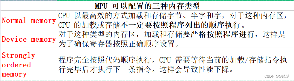
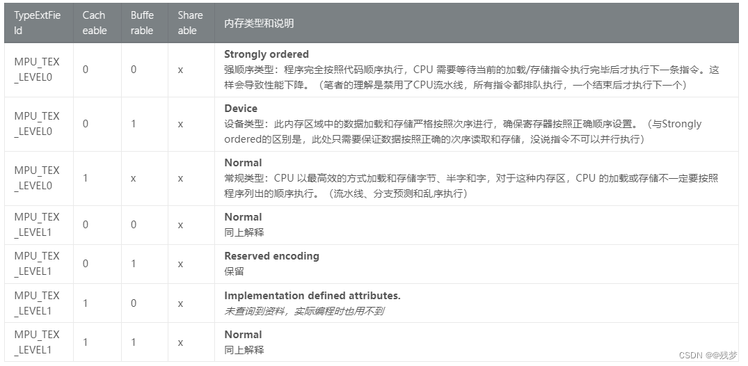
MPU的三种内存类型:
MPU寄存器
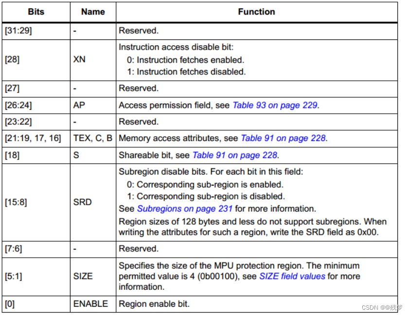
寄存器MPU_RASR
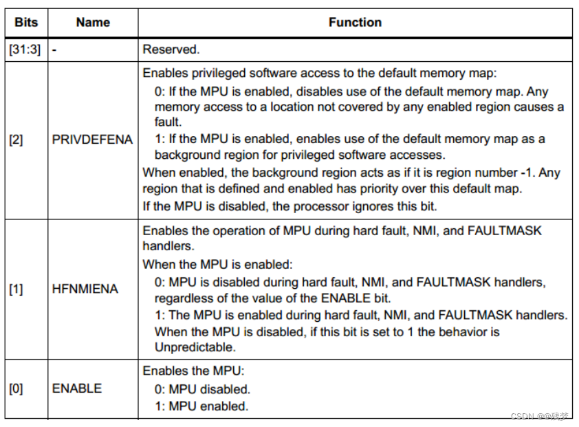
控制寄存器CTRL
HAL库使用MPU时常用的3个函数:
void HAL_MPU_Disable(void)
void HAL_MPU_Enable(uint32_t MPU_Control)
void HAL_MPU_ConfigRegion(MPU_Region_InitTypeDef *MPU_Init)
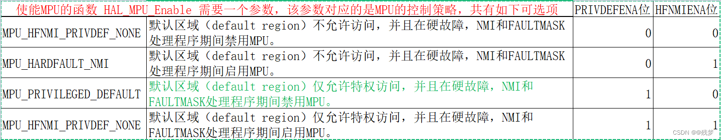
1、void HAL_MPU_Enable(uint32_t MPU_Control)
此函数用于使能 MPU,一般情况使用参数 MPU_PRIVILEGED_DEFAULT。
2、void HAL_MPU_ConfigRegion(MPU_Region_InitTypeDef *MPU_Init)
/ @defgroup CORTEX_MPU_Region_Initialization_Structure_definition MPU Region Initialization Structure Definition* @brief  MPU Region initialization structure* @{*/
typedef struct
{uint8_t                Enable;                /*!< Specifies the status of the region.This parameter can be a value of @ref CORTEX_MPU_Region_Enable                 */uint8_t                Number;                /*!< Specifies the number of the region to protect.This parameter can be a value of @ref CORTEX_MPU_Region_Number                 */uint32_t               BaseAddress;           /*!< Specifies the base address of the region to protect.                           */uint8_t                Size;                  /*!< Specifies the size of the region to protect.This parameter can be a value of @ref CORTEX_MPU_Region_Size                   */uint8_t                SubRegionDisable;      /*!< Specifies the number of the subregion protection to disable.This parameter must be a number between Min_Data = 0x00 and Max_Data = 0xFF    */uint8_t                TypeExtField;          /*!< Specifies the TEX field level.This parameter can be a value of @ref CORTEX_MPU_TEX_Levels                    */uint8_t                AccessPermission;      /*!< Specifies the region access permission type.This parameter can be a value of @ref CORTEX_MPU_Region_Permission_Attributes  */uint8_t                DisableExec;           /*!< Specifies the instruction access status.This parameter can be a value of @ref CORTEX_MPU_Instruction_Access            */uint8_t                IsShareable;           /*!< Specifies the shareability status of the protected region.This parameter can be a value of @ref CORTEX_MPU_Access_Shareable              */uint8_t                IsCacheable;           /*!< Specifies the cacheable status of the region protected.This parameter can be a value of @ref CORTEX_MPU_Access_Cacheable              */uint8_t                IsBufferable;          /*!< Specifies the bufferable status of the protected region.This parameter can be a value of @ref CORTEX_MPU_Access_Bufferable             */
}MPU_Region_InitTypeDef;
示例配置:
MPU_Region_InitTypeDef MPU_InitStruct;/* 禁止 MPU */
HAL_MPU_Disable();/* 配置AXI SRAM的MPU属性为Write back, Read allocate,Write allocate */
MPU_InitStruct.Number           = MPU_REGION_NUMBER0;
MPU_InitStruct.Enable           = MPU_REGION_ENABLE;
MPU_InitStruct.BaseAddress      = 0x24000000;
MPU_InitStruct.Size             = MPU_REGION_SIZE_512KB;
MPU_InitStruct.AccessPermission = MPU_REGION_FULL_ACCESS;
MPU_InitSruct.IsBufferable      = MPU_ACCESS_BUFFERABLE;
MPU_InitStruct.IsCacheable      = MPU_ACCESS_CACHEABLE;
MPU_InitStruct.IsShareable      = MPU_ACCESS_NOT_SHAREABLE;
MPU_InitStruct.TypeExtField     = MPU_TEX_LEVEL1;
MPU_InitStruct.SubRegionDisable = 0x00;
MPU_InitStruct.DisableExec      = MPU_INSTRUCTION_ACCESS_ENABLE;HAL_MPU_ConfigRegion(&MPU_InitStruct);/*使能 MPU */
HAL_MPU_Enable(MPU_PRIVILEGED_DEFAULT);
Number参数:设定当前配置的保护区域编号。此处配置的是0号区域。一共16个区域,0-15
MPU总共有16个可以独立配置的内存保护区域(在CM4内核的MCU中是8个),范围从015。对应的参数就是MPU_REGION_NUMBER0到MPU_REGION_NUMBER15。注意,这些区域编号顺序和其保护的内存区域的顺序无关。也就是说,完全可以配置1号区域为0x240000000x24080000,而2号区域用来保护0x00000000~0x00010000。
MPU保护的区域可以重叠。在发生重叠的时候,优先应用高序号的MPU配置。也就是,序号更大的MPU区域优先级更高。
除了0~15这16个保护区域外,还有一个编号为-1的内存保护区域,其称之为默认区域(default region)或背景区域(background region)。其优先级为最低。默认区域的访问策略由启用MPU的函数HAL_MPU_Enable的参数指定。
Enable参数:此参数用来决定此区域的MPU配置是否启用。
/ @defgroup CORTEX_MPU_Region_Enable CORTEX MPU Region Enable* @{*/
#define  MPU_REGION_ENABLE     ((uint8_t)0x01)
#define  MPU_REGION_DISABLE    ((uint8_t)0x00)
BaseAddress参数、Size参数:此参数用来确定内存保护区域的具体范围
这两个参数在一起确定了内存区域的范围。其中BaseAddress是保护区域的起始地址。Size则是区域的大小。内存区域的起始地址必须对齐到设定的大小。比如将Size设定为1M,那么BaseAddress就必去对齐到1M。即 BaseAddress % Size == 0 。此外,Size是不能随意设置的,只能从 MPU_REGION_SIZE_xxx的宏中进行选取
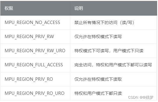
AccessPermission参数:配置此区域的内存访问(读写)权限
SubRegionDisable参数
这个位用于控制内存区的子区域,使用的是 bit[15:8],共计 8 个 bit,一个 bit 控制一个子区域,0表示使能此子区域,1 表示禁止此子区域。一般情况,基本不使用子区域的禁止功能,所以配置 HAL 库的 SubRegionDisable 参数时,直接取值 0x00 即可,表示 8 个子区域均使能。
DisableExec参数:这个参数用来控制当前区域中的指令(代码)是否可以执行
XN=0 表示使能指令提取,即这块内存区可以执行程序代码,XN=1 表示禁止指令提取,即这块内存区禁止执行程序代码。
/ @defgroup CORTEX_MPU_Instruction_Access CORTEX MPU Instruction Access* @{*/
#define  MPU_INSTRUCTION_ACCESS_ENABLE      ((uint8_t)0x00)
#define  MPU_INSTRUCTION_ACCESS_DISABLE     ((uint8_t)0x01)
IsBufferable、IsCacheable、IsShareable、TypeExtField参数:这几个参数组合起来共同决定了所配置的内存区域的缓存和共享策略
MPU_InitStruct.IsBufferable = MPU_ACCESS_BUFFERABLE;MPU_InitStruct.IsCacheable = MPU_ACCESS_CACHEABLE;MPU_InitStruct.IsShareable = MPU_ACCESS_NOT_SHAREABLE;MPU_InitStruct.TypeExtField = MPU_TEX_LEVEL1;
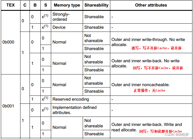
S位用于解决多总线或者多核访问的共享问题,一般不要开启;
TEX = 000表示读开辟,RA; TEX= 001表示读写开辟RWA;
C表示缓存使能标志–cacheable,1表示使能;
B表示bufferable,1表示回写,0表示透写。
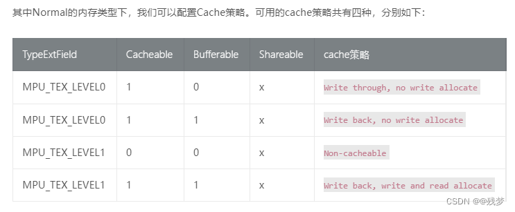
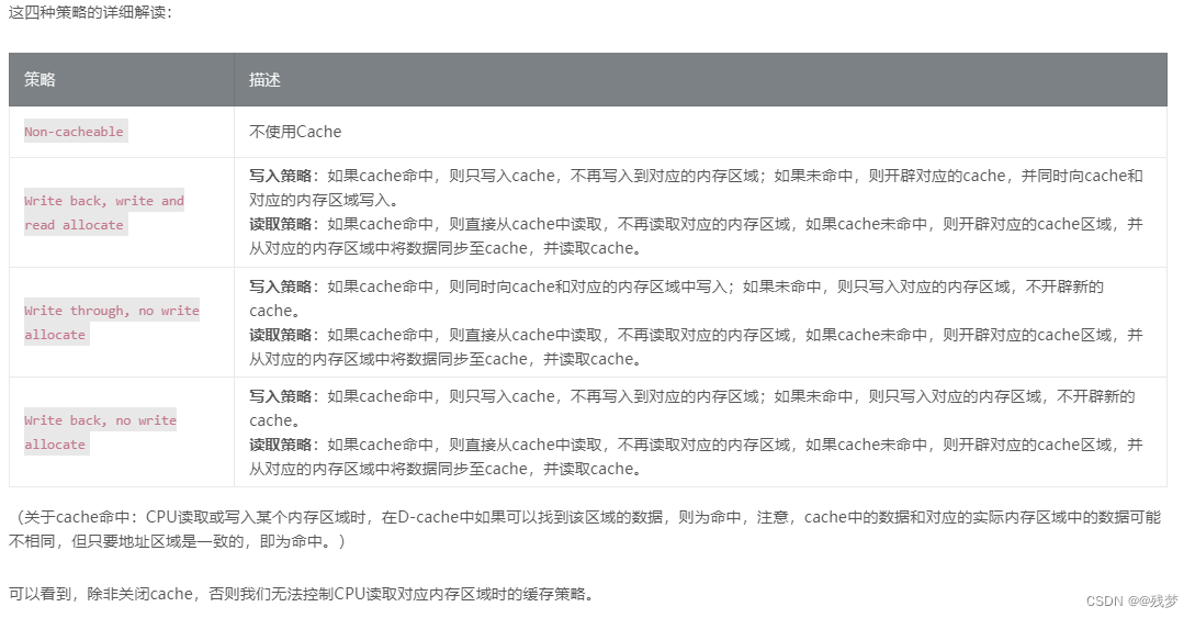
四种Cache( MPU) 配置的读写操作流
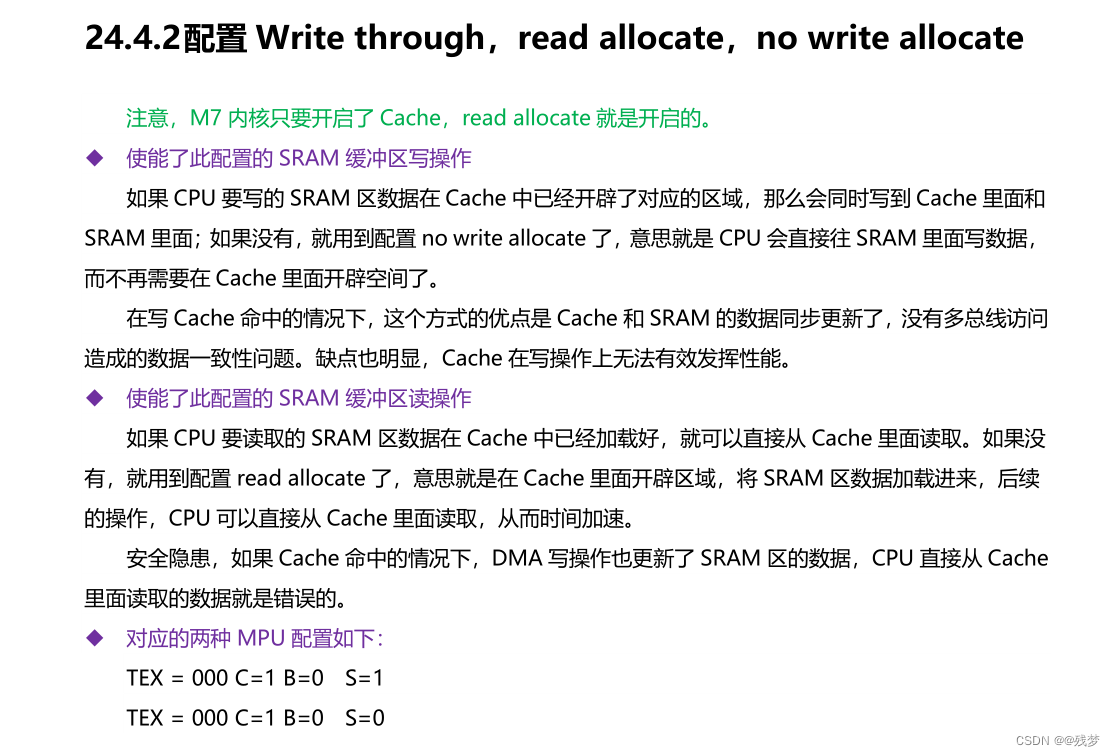
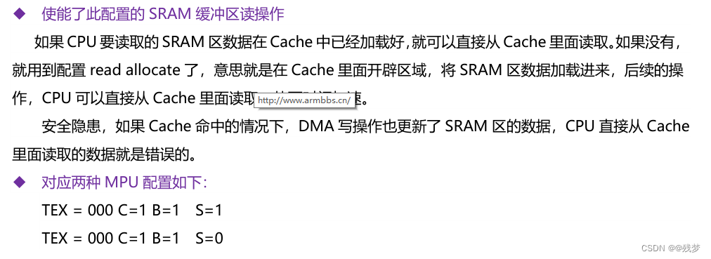
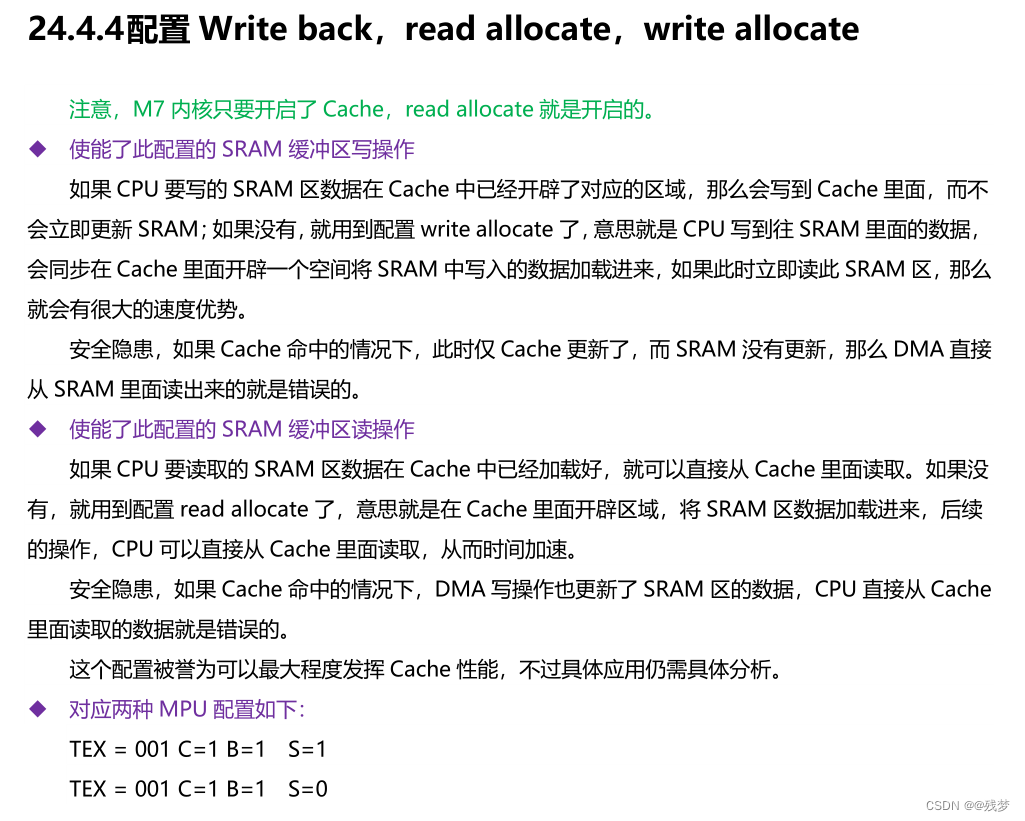
注意,M7 内核只要开启了 Cache,read allocate 就是开启的。
1、配置 Non-cacheable
就是正常的读写操作,无 Cache。

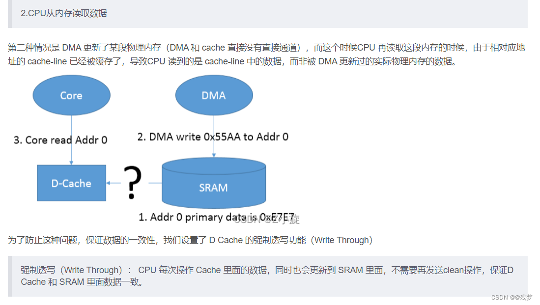
此处可以看看另一篇文章的解释https://blog.csdn.net/qq_28242041/article/details/129582995,方便理解上面为什么说读写错误

透写和回写缓存(Write Through and Write Back in Cache)
透写和回写缓存
高速缓存(Cache)是一种将数据副本临时存储在可快速访问的存储内存中的技术。缓存将最近使用的数据存储在小内存中,以提高访问数据的速度。它充当 RAM 和 CPU 之间的缓冲区,从而提高处理器可用数据的速度。每当处理器想要写入一个字时,它都会检查它想要写入数据的地址是否存在于缓存中。如果地址存在于缓存中,即写入命中(Write Hit)。我们可以更新缓存中的值并避免昂贵的主内存访问。但这会导致数据不一致(Inconsistent Data)问题。由于高速缓存和主存都有不同的数据,如在多处理器系统中,这将导致两个或多个共享主存的设备出现问题。这就是透写(Write Through)和回写(Write Back)出现的地方。
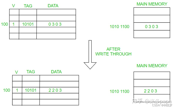
透写(Write Through)
在透写(Write Through)场景中,数据同时更新到缓存和内存(simultaneously updated to cache and memory)。这个过程更简单、更可靠。这用于没有频繁写入缓存的情况(写入操作的次数较少)。
它有助于数据恢复(在断电或系统故障的情况下)。因为我们必须写入两个位置(内存和缓存),数据写入将经历延迟。虽然它解决了不一致的问题,但它的问题是在写操作中使用缓存的优势,因为使用缓存的全部目的是避免对主内存的多次访问。
回写(Write Back)
回写(Write Back)也被称为延迟写入(Write Behind / Write Deferred)。也就是说,最初数据只在缓存中更新,稍后再更新到内存中。对内存的写入动作会被推迟,直到修改的内容在缓存中即将被另一个缓存块替换。
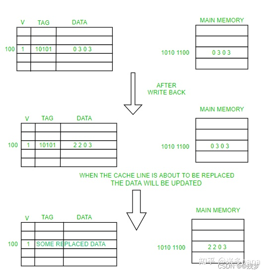
变脏标志位(Dirty Bit):缓存中的每个块都需要一个位来指示缓存中存在的数据是被修改(变脏的)还是未被修改(干净的)。如果它是干净的,则无需将其写入内存。它旨在减少对内存的写操作。如果缓存发生故障(Cache fails)或系统发生故障(System fails)或断电(Power outages),修改后的数据将丢失。因为如果数据丢失了,几乎不可能从缓存中恢复数据。
支持回写的缓存实现起来比较复杂,因为它需要跟踪哪些位置已被覆盖,并将它们标记为变脏,以便稍后写入后备内存中。只有当这些位置的数据从缓存中被逐出时,它们才会被写回后备内存中,这种效果称为延迟写入。出于这个原因,回写缓存中的读取未命中(需要一个块被另一个块替换)通常需要两次内存访问来服务:一次将替换的数据从缓存写回存储,然后一次检索所需的数据。
其他策略也可能触发数据回写。如客户端可能对缓存中的数据进行了多次更改,然后显式通知缓存写回数据。
回写(Write Back)通常与写分配(Write Allocation)一起使用。因为这样不需要将数据从内存中带入缓存,然后再把数据更新缓存和主内存中。同时希望后续写入(甚至读取)到现在已缓存的同一位置。
透写(Write Through)通常与无写分配(No Write Allocate)一起使用。因为它们仍然需要直接写入后备内存,所以在这里后续写入没有优势。
STM32H7内存默认映射和属性
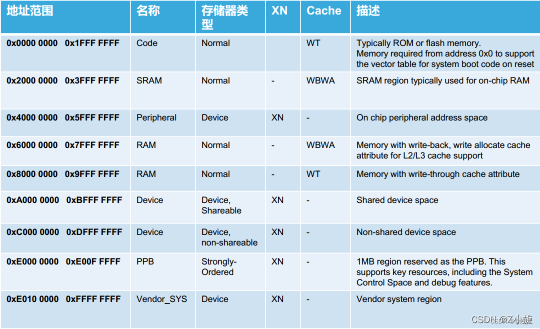
WT 表示 Write-through(透写)
WB 表示 Write-back(回写)
WA 表示 Write-allocate(写分配)
没有明确标注 WA 的就是 RA(读分配)
XN 的意思是 Execute-Never, 其含义为如果相应的地址空间是 XN,是绝不允许执行代码的。
存储器类型为 Normal 的才能使用 cache,并且 TCM 接口是 not cacheable 的。
MPU不配行不行?
在大多数的情况下,如果不访问外部存储空间(如LCD,Flash等),不开启cache的情况下,不配MPU不会有什么问题。但是:
1、H7关闭cache后,性能会有大幅度的下降。
2、由于H7的定位,我们也基本不可能不使用外部存储器。而访问外部存储的内存空间时,如果不配置MPU,则会出现很多奇怪的BUG。比如笔者遇到的FMC
文档参考:
透写和回写缓存(Write Through and Write Back in Cache):https://zhuanlan.zhihu.com/p/571429282
STM32H7/M7中的MPU(内存保护单元)配置详解:https://oshwhub.com/article/STM32H7-M7zhong-de-MPU-nei-cun-bao-hu-dan-yuan-pei-zhi-yang-xie
https://blog.csdn.net/qq_28242041/article/details/129582995
使用STM32H7的FMC注意MPU配置:https://www.armbbs.cn/forum.php?mod=viewthread&tid=89929
STM32H750使用FMC控制LCD数据异常:https://www.stmcu.org.cn/module/forum/forum.php?mod=viewthread&tid=623865&page=1#pid2491693